

measures are taken to prevent solder shorts during Pcb rigid flex
Preventing solder shorts is paramount in the manufacturing of PCB (Printed Circuit Board) rigid flex assemblies to ensure the reliability and functionality of electronic devices. Solder shorts occur when solder bridges form between adjacent conductive elements, such as component leads or PCB traces, leading to unintended electrical connections and potential malfunction or failure of the device. Given the complexity of rigid-flex PCBs, which incorporate both rigid and flexible sections, several measures are taken to mitigate the risk of solder shorts during assembly.
One of the primary measures to prevent solder shorts in pcb rigid flex is meticulous control over solder paste deposition during the stencil printing process. Stencil design parameters, such as aperture size, shape, and spacing, are carefully optimized to ensure precise solder paste deposition onto component pads and PCB traces. Tighter tolerances and smaller apertures help minimize the risk of excess solder paste spreading beyond the intended areas and causing solder shorts between adjacent conductive elements.
Moreover, implementing advanced stencil printing technologies, such as laser-cut stencils or nano-coated stencils, can further improve solder paste transfer efficiency and accuracy, reducing the likelihood of solder shorts. Laser-cut stencils offer superior precision and consistency in aperture dimensions, while nano-coatings reduce solder paste adhesion to the stencil walls, facilitating clean and uniform paste release onto the board substrate.
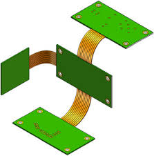
What measures are taken to prevent solder shorts during Pcb rigid flex?
Additionally, employing automated solder paste inspection (SPI) systems can help detect and correct potential issues with solder paste deposition before components are placed onto the board. SPI systems use advanced imaging techniques to analyze the volume, height, and alignment of solder paste deposits, identifying anomalies such as insufficient or excess solder paste, misalignment, or bridging between adjacent pads. By providing real-time feedback to the solder paste printing process, SPI systems help optimize stencil design and printing parameters to minimize the risk of solder shorts.
Furthermore, ensuring proper component placement and alignment on the PCB is critical for preventing solder shorts during assembly. Automated pick-and-place machines use fiducial marks and vision systems to accurately position components relative to the board’s features and ensure proper spacing between adjacent pads or traces. Precise component placement minimizes the risk of solder bridges forming during reflow soldering by maintaining adequate clearance between solderable surfaces and preventing component leads from touching or overlapping.
Moreover, optimizing the reflow soldering process parameters, such as temperature profiles and ramp rates, is essential for preventing solder shorts in PCB rigid flex assemblies. The reflow soldering process involves heating the assembly to a specific temperature to melt the solder paste, followed by controlled cooling to solidify the solder joints. Proper temperature profiling ensures that the solder paste reaches its melting temperature uniformly across the entire assembly, allowing for consistent wetting and solder joint formation without overheating or causing solder migration between adjacent conductive elements.
In addition to process control measures, post-soldering inspection and testing are essential for detecting and rectifying any solder shorts that may have occurred during assembly. Automated optical inspection (AOI) systems and X-ray inspection techniques can be used to inspect solder joints for anomalies such as solder bridges, insufficient solder, or misalignment. Any detected defects can be addressed through rework or repair processes to ensure the integrity and reliability of the PCB assembly.
In conclusion, preventing solder shorts in PCB rigid flex assemblies requires a comprehensive approach that addresses stencil design, solder paste deposition, component placement, reflow soldering processes, and post-soldering inspection and testing. By implementing measures such as optimized stencil design, precise component placement, controlled reflow soldering parameters, and thorough inspection techniques, electronics manufacturers can minimize the risk of solder shorts and ensure the reliability and functionality of rigid-flex PCB assemblies.