

RF PCBs ensure low-loss transmission
Ensuring low-loss transmission is a critical design goal for RF (Radio Frequency) PCBs (Printed Circuit Boards), as even small signal losses can significantly degrade the performance of high-frequency systems. RF PCBs are used in a wide range of applications, including telecommunications, radar systems, and wireless communication, where signal integrity is crucial. Signal loss in these systems can lead to reduced range, interference, and compromised data transmission. To maintain optimal performance, RF PCBs employ various design strategies and materials to minimize signal attenuation, ensuring low-loss transmission. In this article, we will explore how RF PCBs achieve low-loss transmission by focusing on material selection, transmission line design, impedance matching, and other critical design considerations.
The first and most significant factor in achieving low-loss transmission in rf pcb is the choice of materials. The dielectric properties of PCB materials directly affect signal loss. Materials with low dielectric constants (Er) and low loss tangents (tan δ) are essential for reducing signal attenuation. The dielectric constant influences the speed at which signals travel through the PCB, while the loss tangent represents the amount of energy dissipated as heat. High-loss materials can absorb RF energy, leading to increased signal attenuation. Therefore, RF PCBs often use advanced materials such as PTFE (polytetrafluoroethylene), Rogers laminates, or other specialized composites that have low loss tangents and stable dielectric constants at high frequencies. These materials help preserve signal strength, ensuring that RF signals experience minimal attenuation as they travel through the board.
In addition to material selection, the design of the transmission lines within the RF PCB plays a crucial role in reducing signal loss. RF signals typically travel along transmission lines such as microstrip, stripline, or coplanar waveguides. These transmission lines must be carefully designed to maintain consistent impedance and minimize the losses caused by reflections and power dissipation.
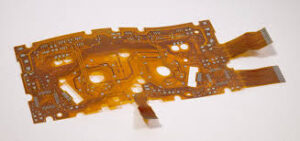
How do RF PCBs ensure low-loss transmission?
A mismatch in impedance between the transmission line and the connected components (such as antennas or amplifiers) can cause signal reflections, which waste energy and reduce signal strength. To avoid this, PCB designers ensure that the impedance of the transmission line is controlled and uniform across the entire signal path. This is achieved by adjusting trace widths, the distance between traces and ground planes, and the overall layer stack-up. The goal is to design transmission lines that minimize reflections and power losses, ensuring efficient signal transmission.
The next important consideration in ensuring low-loss transmission is impedance matching. Impedance matching is critical in RF circuits because any mismatch can cause signal reflections, which lead to energy loss and distortion. Inductors, capacitors, and resistors are used in conjunction with transmission lines to match the impedance of various components and maintain signal integrity. RF PCBs often employ techniques such as microstrip lines or stripline configurations to control impedance at different points in the circuit. These methods help ensure that signals are transmitted smoothly without unwanted reflections or losses, thereby improving the efficiency of the system.
Another key factor in minimizing signal loss is the careful design of vias and their placement. Vias are used to connect different layers of the PCB, but poorly designed or long vias can increase inductance and resistance, leading to signal degradation. In RF circuits, vias should be as short and direct as possible to minimize their impact on signal integrity. Using advanced via technologies such as blind or buried vias, as well as via-in-pad designs, can help reduce the negative effects of vias on signal loss. Additionally, via plating must be done properly to ensure that the signal’s path remains low-loss and high-performance.
Grounding is also a critical aspect of minimizing signal loss in RF PCBs. A solid and continuous ground plane is essential to provide a stable reference for the signal and to reduce electromagnetic interference (EMI). A poor grounding system can lead to noisy signals, which increase attenuation and disrupt signal transmission. RF PCBs often incorporate solid copper ground planes and use via stitching between the layers to create a continuous grounding network. This not only improves signal integrity but also reduces the likelihood of noise coupling into the signal path.
Thermal management is another consideration that indirectly impacts signal loss in RF PCBs. Excessive heat can increase the resistance of components and materials, leading to higher signal loss. Proper thermal management techniques, such as heat sinks, copper pours, and thermal vias, help dissipate heat and maintain the integrity of the signal. By preventing overheating, designers ensure that the PCB operates at optimal temperatures, thereby reducing the likelihood of performance degradation due to thermal effects.