
Micro Via Be Recycled
If you’re a PCB designer, a micro via is an essential tool for creating compact, high-density circuit boards. They enable you to route signals and power across multiple layers while maintaining the required minimum trace width. In order to effectively utilize microvias, it’s important to understand the process behind them. Stacked microvias are a particular concern, as they require special consideration and testing to ensure that the design is robust and reliable.
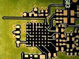
A microvia is a laser-drilled hole that interconnects one layer with the next in the stack-up. It’s possible to drill a microvia mechanically, but it’s more efficient and cost-effective to use a laser for this purpose. Unlike standard vias, which are cylindrical in shape, microvias have a conical frustum shape. Their walls slope inward to connect with a pad on the layer immediately below them. This structure is ideal for forming connections across multiple layers, but it can present reliability concerns when stacked in a matrix.
The most common micro via failure mode involves the copper plating that fills a via. If the plated copper has an uneven thickness, it can create stress at the interfaces where adjacent vias are stacked together. This can lead to stress concentration around the edges of the void, which may cause it to crack or dimple. The best way to avoid this problem is by using a laser for the drilling of your microvias. The precision achieved by a laser also reduces the likelihood of manufacturing defects like voids, dimples, or bumps.
Can Micro Via Be Recycled?
Another issue with a stacked microvia is that it can result in a shorter, unterminated signal pathway. This is because the unused portion of copper barrel in the via stub can cause reflections when the signal switches at high speeds. This is especially a problem with the copper in the knee (where the microvia slopes into the top pad).
When a stacked microvia is fabricated, it’s important to minimize its height and length to maintain a reasonable balance between the mechanical integrity of the board and its electrical performance. This is why a laser is used for drilling microvias, which helps to ensure that the copper has an even thickness.
The final steps in defining microvias include building a proposed stackup in the PCB designer software and ensuring that the stackup can be fabricated with the selected materials. This is best done by sending the stackup to your PCB fabricator for review and their input on manufacturability with microvias. By taking the time to define the correct stackup and discuss any fabrication concerns with your fabricator, you can ensure that your design will be able to benefit from the advantages of this innovative technology.
To ensure that your stacked microvias are fabricated properly, you should work closely with your board fabricator to determine the optimal layer-pair and stack-up. This will help you to avoid potential issues with your stacked microvias and achieve the highest levels of reliability in your finished product. Having this information at hand will allow you to confidently place your orders and prepare for manufacturing.